 |
8-5: The Layer Cells |
|
|
8-5: The Layer Cells |
|
To edit an existing layer, use the Edit Layer... command of the Technology menu, and to create a new layer use the New Layer... subcommand of the New Primitive command. Once a layer is being edited, the next one in sequence can be edited with the Edit Next Primitive command. The current layer can be deleted with Delete this Primitive. Also, you can rename a layer with the Edit Cell... command of the Cells menu, but remember to use the name "layer-" in front (i.e. the old name is "layer-metal" and the new name is "layer-metal-1"). Finally, you can rearrange the order in which the layers will be listed by using the Reorder Layers subcommand of the Reorder Primitives command.
| There are many pieces of information in a layer, most of which can be updated by highlighting them and using the technology edit button. There is a 16x16 stipple pattern, a large square of color above that, and a number of pieces of textual information along the right side. |  |
The stipple pattern can be changed simply by selecting any grid squares and then using the technology edit button. You can also do operations on the entire stipple pattern by clicking on the text "Stipple Pattern Operations" and using the technology edit button. These operations include clearing the pattern, inverting the pattern, copying, and pasting the pattern (between layers).
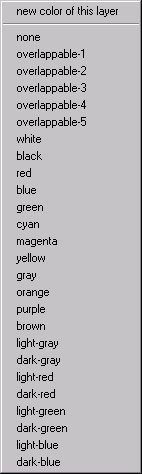 |
The color of the layer can be changed by highlighting the "Color"
entry on the right and using the
technology edit button.
A menu then proposes five transparent and many named (opaque) colors.
Transparent colors have a unique appearance when they overlap each other, as defined in the technology's color map. The named colors are opaque, so they obscure anything under them when drawn. In general, the five most commonly used layers should be assigned to the five transparent colors, and the remaining layers should have opaque color. See Section 4-6 for more information on color. The "Style" entry on the right can be "solid", "patterned", or "patterned/outline" to indicate how that layer will be appear. When using "solid" styles, the 16x16 stipple pattern is ignored (except for hardcopy). The "patterned/outline" option draws a solid line around all patterned polygons. Transparent layers should be solid because they distinguish themselves in the color map. Layers with opaque colors should probably be patterned so that their combination is visible. |
The "Print colors" at the bottom are used when producing PostScript that is "Color Merged" (see the Print Options... command of the File menu). The first three numbers are the red, green, and blue. The next number is an opacity, from 100 (fully opaque) to 0 (transparent). The last factor is a "foreground" flag which, when "on" indicates that the non-opaque colors can be combined with others.
Many of the entries on the right side of the layer cell provide correspondences between a layer and various interchange standards. The "CIF Layer" entry is the string to use for CIF I/O. The "DXF Layer" entry is the string to use for DXF I/O. The "GDS-II layer" is a single number (-1 when there is no layer).
The "Function" entry allows a general-purpose description to be attached to the layer.
A function can be only 1 of the values from this table.
However, the last 12 entries are additional attributes that can combine with the layer function to further describe it:
For example, you can highlight the function entry and use the technology edit button many times, selecting "Diffusion", "p-type", and "heavy" to indicate a Diffusion layer that is heavily-doped p-type. To clear the layer function, set it to "unknown." There must be a "pseudo" layer for every layer used to build arcs. This is because every arc needs a pin, and pins are constructed with "pseudo" layers. The "pseudo" layers are "virtual" geometry that do not appear in the fabrication output. It is important that every "pseudo" layer have an associated real layer, with similar descriptive fields. The technology editor will issue a warning if pins are not constructed from pseudo-layers. |  |
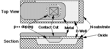
Note that the layer functions must be treated carefully as they form the basis of subsequent arc and node definitions. One consideration to note is the use of "Wells" and their significance to the SPICE extractor. If the technology requires a separate contact to the well, then it will typically contain a metal layer, and a piece of heavily doped material under the metal to make ohmic contact to the well; i.e. p++ in a P-well. This will have the same doping as the well, unlike a device diffusion, which is of opposite type to the well in which it is located.
Two rules apply here: (1) there must be a separate diffusion layer for the p++ or n++ used as a contact in a P-well or N-well, respectively; it cannot be the same layer that is used for diffusions in active devices; and (2) a p++ or n++ layer that is used to make a contact in a well of the same semiconductor type (for example p++ in a P-well) must not be defined with the layer function Diffusion; it must be declared as "Well". In the well contact shown below, both the p++ layer and the P-well layer will be defined with the layer function "Well, P-type".
The "Layer letters" field is one letter (or at most two) that uniquely identify this layer. You must not place the same letter in this field on two different layers. These letters are used as abbreviations for the layers in some internal commands, but have no meaning to the average user. Nevertheless, it is best to keep track of which letter has been used with each layer to prevent duplication.
Another set of options on the right side of the layer cell is for SPICE parasitics. You may assign a resistance, capacitance, and edge capacitance to the layer for use in creating SPICE simulation decks. If a layer has nonzero edge capacitance, it must also have nonzero capacitance, because the extractor checks the capacitance value to decide whether to include the layer in parasitic computations. This is true even if the layer is used in an arc that contains device diffusion; the extractor will correctly cancel out the capacitance, and include the edge capacitance in the extraction process.
The "3D Height" and "3D Thickness" are used when viewing a chip in 3-dimensions. The height and thickness are arbitrary values (usually a small integer). They indicate the location and thickness in the third axis (out of the screen). For example, to show how poly and diffusion interact, the poly layer can be at height 21 and the diffusion layer at height 20, both with 0 thickness. This will appear as two ribbons, one over the other. Use the 3D Display commands of the Windows menu to see a 3-dimensional view of the circuit.
 |
Previous |  |
Table of Contents | Next |  |