 |
9-3: Electrical-Rule Checking |
|
|
9-3: Electrical-Rule Checking |
|
To check the well and substrate layers, use the Analyze Wells subcommand of the Electrical Rules command of the Tools menu. This does a more thorough job of checking the layers than the design-rule checker. This may take some time, and if it takes too long, you can abort it with the interrupt key (see Section 1-9).
After analysis is done, you can review the errors by typing ">" to see the next error and "<" to see the previous error. You can also see the list of errors in the Cell Explorer (see Section 3-7).
| The Well Checker makes sure that there are well contacts in every area of well. You can relax this restriction with the Well Check Options... command. This dialog allows you to request that there be only 1 well contact, anywhere on the chip. You can also instruct the checker to ignore contacts entirely. | 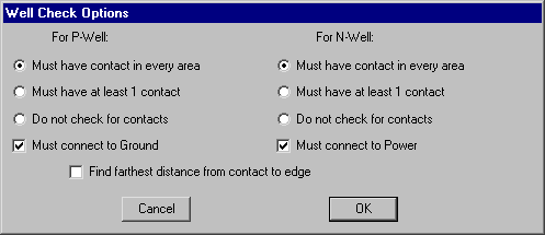 |
The Well Checker also checks spacing rules between well areas. Although this is generally the domain of the Design Rule Checker, it is not done there, so it is done here.
The Well Checker also checks that there is a connection to power and ground in the appropriate places. You can disable these checks in the Well Check Options... dialog.
An additional well check is to find the farthest distance from a substrate contact to the edge of that area. This check takes more time to do.
Finally, the Well Checker reports the maximum distance from a well contact to any point on the well. This is useful when making sure that there are sufficient contacts for each area.
Antenna rules are required by some IC manufacturers to ensure that the transistors of the chip are not destroyed during fabrication. During fabrication, the wafer is bombarded with ions during the polysilicon and metal layer creation process. These ions must find a path to through the wafer (to the substrate and active layers at the bottom). If there is a large area of poly or metal, and if it connects ONLY to gates of transistors (not to source or drain or any other active material) then these ions will travel through the transistors. If the ratio of the poly or metal layers to the area of the transistors is too large, the transistors will be destroyed.
To check for antenna rule violations, use the Antenna-Rules Check subcommand of the Electrical Rules command of the Tools menu. After analysis is done, you can review the errors by typing ">" to see the next error and "<" to see the previous error. You can also see the list of errors in the Cell Explorer (see Section 3-7).
| To modify the required ratio of poly or metal to transistor area, use the Antenna-Rules Options... subcommand. | 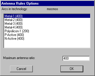 |
 |
Previous |  |
Table of Contents | Next |  |