 |
9-2: Design-Rule Checking |
|
|
9-2: Design-Rule Checking |
|
Three types of errors are detected by the incremental and hierarchical design-rule checkers. Spacing errors are caused by geometry that is too close, but not connected. Notch errors are caused by geometry that is too close, but connected. Minimum size errors are caused by geometry that is too small.
In addition to examining geometry, the design-rule checkers use connectivity information to help find violations. This use of network information helps the designer to debug circuit connectivity. For example, if two overlapping nodes are not joined by an arc, they may be considered to be in violation, even if their geometry looks right. This is because the checkers know what is connected and have a separate set of rules for such situations.
The incremental design-rule checker is always running, examining your work, and issuing error messages when an error is detected. The user should be warned that the incremental design-rule checker does not examine hierarchy. This means that if a cell instance is used in a circuit, the incremental design-rule checker does not examine its contents to see how that interacts with other layout surrounding the instance. To check the complete hierarchy, use the Check Hierarchically subcommand.
To control the DRC, use the DRC Options... subcommand of the DRC command of the Tools menu.
|
By default, the incremental design-rule checker is on.
To turn it off, uncheck the "On" checkbox in the "Incremental DRC" section.
While the tool is off, Electric keeps track of all cells that change.
When the tool is turned back on it rechecks all of those changed cells.
Thus, the incremental design-rule checker can be made into a "batch" tool by keeping it off until circuit layout is complete.
MOS contact nodes automatically increase the number of cuts when they grow larger (see Section 7-4). Because of this, very large contact nodes can create excessive work for the design-rule checker as it examines each of the cuts. To save time, check the "Ignore center cuts in large contacts" check box, which will examine only the cut layers around the edges of contact nodes.
|  |
After errors have been reported, you can review them by typing ">" and "<" to step to the next and previous error that was found. If you wish to recheck an entire cell, use the Check this Level Only subcommand.
The hierarchical design-rule checker uses the same rules and techniques as the incremental checker, but it is able to check across levels of hierarchy. To run it, use the Check Hierarchically subcommand of the DRC command of the Tools menu. To check only a selected subset of the current cell, use Check Selection Area Hierarchically.
To help guide the design-rule checker, a "cloaking" layer can be placed over areas that are not to be examined. This cloaking layer is created by using the DRC Exclusion subcommand of the New Special Object command of the Edit menu. Any errors that fall inside of this node's area are ignored.
After analysis of the circuit, you can review the errors by typing ">" and "<" to step to the next and previous error that was found. You can also see a list of errors in the Cell Explorer (see Section 3-7).
After a cell has passed Hierarchical DRC with no errors, it is tagged with the current date. In subsequent runs of the Hierarchical DRC, if the cell has not been modified since that date, it is not rechecked. (However, if you change the DRC rules or the technology options, all date information is cleared.) If you wish to force all cells to be rechecked, use the "Clear valid DRC dates" button in the DRC Options... dialog. To see which cells have passed Hierarchical DRC, use the General Cell Lists... command of the Cells menu (a "D" is shown in on the right for cells that are DRC current).
Another way to speed up Hierarchical DRC is to check the "Just 1 error per cell" entry in the DRC Options... dialog. This tells the system to stop checking a cell after the first error has been found. By using this option, you can more quickly determine which cells in the design are correct, without knowing exactly where the errors lie. Then, you can go to the cells with errors and do a more complete check.
If you are fortunate enough to have a computer with more than 1 processor, the DRC can take advantage of this when doing hierarchical checking. Check "Use multiple processors" in the DRC Options... dialog and tell it how many processors to use. The value of this field sets the number of parallel threads that will be spawned to do the DRC, so it can be more than the number of processors.
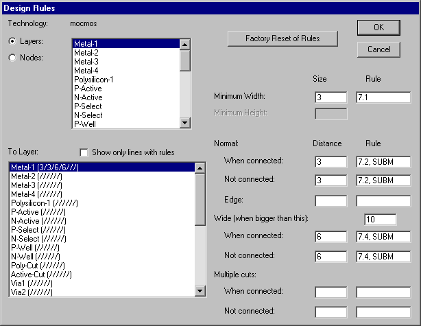
The DRC Rules... dialog allows you to examine and modify the spacing limits for the current technology. You can select "Layers" or "Nodes". When "Nodes" are selected, you may set the minimum size of each node in the current technology.
When "Layers" are selected, you may set the minimum size of each layer as well as inter-layer spacing (between that and the "To Layer"). Use the "Show only lines with rules" to restrict the displayed rules to those with valid values. Each spacing rule comes in two flavors: connected and unconnected. The connected rules apply to two different layers that are electrically connected; the unconnected rules apply to unconnected layers. A special Edge rule applies only to unconnected layers and ignores overlap when considering spacing distance. The connected and unconnected rules come in three styles: normal, wide, and multiple cut. The Wide rules apply when either layer is wider than a specified amount. The Multiple cut rules apply when either layer is part of a multi-cut contact. In addition to specifying a spacing distance, you can give a description of the rule that will be reported by the design-rule checker. The "Factory Reset of Rules" button restores all rules to the original set built into Electric.
Note that the MOSIS CMOS design rule 6.7b is not checked by Electric because it is difficult to detect properly. This error is never fatal, and the worst case of missing this error is that active and poly are closer by 1/2 lambda, which merely results in an increase in capacitive coupling between them. If this fringing capacitance is important, you've probably got so much polysilicon in your circuit that it has bigger problems.
Another design-rule checking facility that is available in Electric is an interface with the Dracula design-rule checker. This interface requires a circuit description and a set of design rules. Electric knows the design-rules (currently only for the MOSIS CMOS technology) and is able to generate the proper circuit description (a CIF file). To generate these files, use the Write Dracula Deck subcommand.
To see the set of Dracula design rules for the current technology, use the "Edit Dracula Deck" button of the DRC Options... subcommand. This will display the rules in an edit window. The rules must contain the lines: "PRIMARY =" and "INDISK = " so that the deck generator can substitute the proper file names.
Note that only the "mocmos" technology has valid design rules, so this command will present an empty window when run in other technologies. However, you can create your own design-rules for any technology. To do this, follow these steps:
To help guide the Dracula design-rule checker, a "cloaking" layer can be placed over areas that are not to be examined. This cloaking layer is created by using the DRC Exclusion subcommand of the New Special Object command of the Edit menu. The node that is placed produces a layer called "DRC" in the Dracula file, which causes the circuitry underneath to be ignored.
 |
Previous |  |
Table of Contents | Next |  |