
Chapter 8: Creating New Technologies
|
8-6: The Node Cells | |
Nodes are the components in a technology, and they are constructed from pieces of geometry on the layers. To edit an existing node, select it from the cell explorer or the Edit Cell... command (in menu Edit).
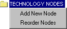 | To create a new node, use the context menu on the "TECHNOLOGY NODES" entry of the cell explorer and choose "Add New Node". |
A node can be deleted simply by deleting its cell. A node can be renamed by renaming its cell, but remember to use the name "node-" in front (i.e. the old name is "node-metal" and the new name is "node-metal-1"). Finally, you can rearrange the order in which the nodes will be listed with the "Reorder Nodes" command from the context menu.
|
The node cell contains four pictures of the node on the bottom and textual information above that.
You can update the textual information entries by double-clicking on them.
The "Serpentine transistor" entry indicates that this is a MOS transistor and it can take arbitrary outline information to describe its geometry (see Section 7-4-1). The "Square" entry forces the node to always have the same X and Y dimension when scaled. | 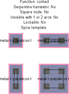 |
The "Invisible with 1 or 2 arcs" entry indicates that the node will not be drawn if it is connected to exactly one or two arcs. This is useful in schematic pins, which are visible only when unconnected or forming a junction of 3 or more wires.
The "Lockable" entry indicates that this node can be made unchangeable along with other lockable primitives, when the lock is turned on during editing (see Section 6-2 for more on locking these primitives). This is typically used in array technologies such as FPGA (see Section 7-6-2).
The "Spice template" entry is an overriding line of Spice code to be emitted for this primitive. See Section 9-4-4 for more on Spice templates.
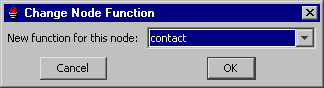 | The "Function" entry describes the node's function, which is a different set than the arc and layer functions. A dialog offers a list of possible node functions. |
For nodes, it is common to sketch four different examples of the node in varying scales, so that X and Y scaling rules can be derived (square nodes need only two examples). If only one example is specified, linear scaling rules will be presumed.
The smallest example, called the main example, is used as the default size and also contains all of the special port information. Needless to say, it is important to keep the geometry of each example well apart from the others so that the technology editor can distinguish them.
Each example must contain the same geometric layers (only stretched). As in the Arc cells, pieces of geometry can be created by selecting from the component menu of the side bar, creating the geometry, and then double-clicking to assign a layer. If any polygonal geometry is used (for example, the Filled polygon entry, sixth from the top), they require outline information to be assigned (see Section 6-10-1). If the Opened circle arc entry is selected (second from the bottom), you can specify the number of degrees of the circle with the Object Properties... command (in menu Edit / Properties).
Each example must also contain a highlight layer to indicate the correct highlighting on the display. Select the "HIGH" entry from the component menu to create this special type of layer.
Each example must also contain port information. Select the "PORT" entry in the component menu to create this special type of layer. You will have to provide a name for each port, and the name must be the same on each example.
|
Ports on the main example must also have connectivity information (which arcs can connect to them) and range information (the permissible angle of connected arcs). Double-click on the port to set this. The range consists of two numbers: an angle (in degrees counterclockwise from 3 O'clock) and an angle range. For example, a port angle of 90 with a port angle range of 45 describes a port that points upward and can connect at angles up to 45 degrees off from this direction. The range will be graphically depicted. | 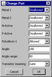 |
The ports on the main example must also indicate any internal electrical connectivity by actually connecting them together. For example, the two polysilicon ports on a MOS transistor should be connected in the main example. Join the ports with a universal arc. Do not put this internal connection on any example other than the main one. To see the location of all ports on the main example, use the Identify Ports command (in menu Edit / Technology Editing).
For simple nodes, such as pins and contacts, there is typically one port which is in the center of the node. However, some of Electric's built-in technologies give these ports a nonzero size. The idea behind doing this is to allow arcs to "slide" within that port (see Section 5-2-2). Many disagree with the idea of having nonzero ports on pin nodes, and so it is now recommended that all pin nodes have zero size ports.
As with arcs, use the Identify Primitive Layers command to label each piece of geometry in the main example.
It is sometimes the case that two or more primitive nodes are nearly the same and differ only by the shape of their layers. When this happens, it is possible to define them all in the same cell using the notion of variations. To create a variation on a node, create a 5th example in the cell (for two variations, create a 5th and 6th example). Each variation example must follow these rules:
| 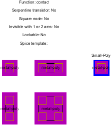 |
The picture shown here illustrates a variation in which the polysilicon layer is inset. The text "Small-Poly" is the name of the cut node (moved up to make it readable).
There are some special cases available in node descriptions. A piece of geometry in the main example may be changed (by double-clicking on its function) to "SET-MINIMUM-SIZE". This indicates that the current size is the smallest possible, and it cannot scale any smaller (this is used by the "mocmos" technology for the metal layer in contacts). The restriction can be removed with the "CLEAR-MINIMUM-SIZE" description. This option cannot be used in serpentine transistors.
Another special case in node description is the ability to specify multiple cut layers. If the larger examples have more cut layers, rules are derived for cut spacing and indentation so that an arbitrary numbers of cuts can be inserted as the contact scales.
Although serpentine MOS transistors are a special case, they cannot be automatically identified, but must be explicitly indicated with a textual indicator. Besides this explicit indication, the transistor node must contain four ports: two on the gate layer (polysilicon) and two on the gated layer (active). A standard geometry must be used that shows polysilicon and diffusion crossing in a central transistor area. Any deviation from this format may cause the technology editor to be unable to derive serpentine rules for the node.
Besides the standard nodes for transistors, contacts, and other circuit elements, it is necessary to build pin and pure-layer nodes. There should be one pin for every arc, so that the arc can connect to others of its type. The pin should be constructed of pseudo-layers (i.e. it has no real geometry), should have the "pin" function, and should have one port in the center that connects to one arc. The technology editor will issue a warning if there is no pin node associated with an arc.
The pure-layer nodes should also be built, one for each layer. They should have only one piece of geometry and have the "pure-layer" function. The technology editor will issue a warning if there is no pure-layer node associated with a layer.
 |
Previous |  |
Table of Contents | Next |  |