Chapter 8: Creating New Technologies
 |
8-10: Technology XML File Format |
|
Introduction
Layout technologies in Electric can be described by Xml technology files.
These files are automatically generated by the technology editor and the technology-creation wizard,
but some users may prefer to edit them by hand.
For these users, the following is a description of the technology XML file format.
Electric currently has Xml technology files that are unparameterized
(all values are explicitly entered and there is no symbolic information).
Technology distances are specified as double-precision numbers in display units.
Future versions of Electric may implement a symbolic style of Xml technology files.
Currently technology files contain two kinds of information:
- Electric-independent information.
This includes physical and electrical details of the foundry process.
Most of these details are attached to Layers and includes
design rules, simulation information, etc.
- Electric-specific information.
This includes the primitive nodes and arcs that Electric uses for design.
It also has connectivity rules, display and print styles,
component menus for the technology, etc.
Primitive nodes and arcs can be considered to be layout macros.
Node description consists of a set of two-dimensional shapes.
Arcs description consists of a set of one-dimensional intervals, which are stretched in the other dimension.
The technology file describes primitive nodes and arcs of a standard size (usually
the DRC minimum) and also includes information about how they can grow larger.
Instances of these nodes and arcs in Libraries can be larger than standard.
A primitive node or arc can consists of many shapes in different technology Layers.
Each shape in a primitive node is called a NodeLayer.
Each interval in a primitive arc is called an ArcLayer.
The minimum bounding box of all NodeLayers of a primitive node is called its FullRectangle.
Description of a primitive node can also define the FullRectangle explicitly.
The largest of all ArcLayers in a primitive arc defines its FullWidth.
Primitive nodes and arcs also have the notion of a BaseRectangle and a BaseWidth.
They relate to the shape of the most important layer in this node or arc.
The BaseRectangle of a primitive node is described explicitly.
The BaseWidth of primitive arc is the width of the first 'ArcLayer' in the arc description.
The BaseRectangle and BaseWidth are highlighted in the Edit Window and they appear
in Properties dialogs.
Instances of nodes and arcs in a library can have sizes larger than standard.
Electric writes size information of each instance in the library files.
Since release 8.05 of Electric (or more precisely since the 8.05o development version)
library files contain the extent of the node/arc over its standard size
described in the technology file. When you switch a design library from one technology
to another compatible technology, the standard size node/arc in old technology is
converted to the standard size node/arc in the new technology. The node/arc which extends
by 1 unit beyond the standard node/arc in old technology is converted to a node/arc which
extends by 1 unit beyond the standard node/arc in new technology.
Older Electric releases wrote sizes of node/arc instances in another way.
Jelib format before Electric 8.05 (actually, the 8.05g development version) and all Elib files
saved the size of the FullRectangle and FullWidth.
Jelib format between 8.05g and 8.05n wrote sizes of BaseRectangle and BaseWidth.
The Full and Base sizes can be redefined in future versions of technology file.
To be able to read older Jelib formats correctly after redefinition of Full and Base,
Technology file can contain explicit sizes of standard nodes and arcs in older library files.
All sizes in technology files are in display units.
There is a scale declaration which relates this unit to nanometers.
Overall Structure
Here is a description of Xml technology file in Electric releases 8.05 and 8.06.
<technology> is the main element of the Xml technology file. It has many Xml-specific attributes:
-
"name" contains the name of this technology inside Electric.
-
"class" (optional) contains the name of a Java class which is a subclass of "com.sun.electric.technology.Technology".
It can be used to describe things which are not described by the Xml technology class yet.
The interface with this class is not specified and can be changed.
If you need a non-standard technology feature, the better way is to contact Electric developers about this.
Example:
   <technology name="mocmos"

      class="com.sun.electric.technology.technologies.MoCMOS"

      xmlns="https://electric.sun.com/Technology"

      xmlns:xsi="https://www.w3.org/2001/XMLSchema-instance"

      xsi:schemaLocation="https://electric.sun.com/Technology

         ../../technology/Technology.xsd">
Inside of the <technology> element are these subelements:
-
<shortName> a more descriptive name for the technology (optional)
-
<description> the most descriptive name for the technology.
-
<version> describes Electric versions when Jelib changed and how it affects sizes.
The "tech" attribute contains an identifier of this version used in subsequent <diskOffset> subelements
of <arcProto> and <primitiveNode> descriptions. The "electric" attribute is a corresponding Electric version.
These elements are usually fixed in all technology files.
Examples:
   <version tech="1" electric="8.05g"/>

       <version tech="2" electric="8.05o"/>
-
<numMetals> describes a possible range for the number of metall layers in the technology.
There is no good support for Xml technology files with a variable number of metal layers.
Therefore, this element should contains the same value for all three attributes.
Example:
<numMetals min="6" max="6" default="6"/>
-
<scale> defines how many nanometers are in a display unit.
Electric uses dimensionless "units" in its interface, where a transistor may be "2x3"
without specifying actual distances. This scale converts the units to real spacings.
The "relevant" attribute should be true for layout technologies.
Example:
<scale value="200.0" relevant="true"/>
-
<resolution> defines the minimum resolution value in grid units used in DRC,
a parameter to determine which points are off-grid.
Example:
<resolution value="2.0"/>
-
<defaultFoundry> is a name of the default foundry for this technology.
The name references one of the <foundry> elements found later in the Xml file.
Example:
<defaultFoundry value="MOSIS"/>
-
<minResistance> global minimum resistance (for parasitics).
Example:
<minResistance value="4.0"/>
-
<minCapacitance> global minimum capacitance (for parasitics).
Example:
<minCapacitance value="0.1"/>
-
<logicalEffort> defines default project preferences for the Logical Effort tool.
Example:
   <logicalEffort gateCapacitance="0.167" wireRatio="0.16"

	      diffAlpha="0.7"/>
-
<transparentLayer> defines the transparent layers in the technology. All layers can be drawn
in either a "transparent" or "opaque" style. Transparent layers can overlap other transparent
layers without obscuring each other (they blend where they overlap). Opaque layers cover all
other layers without blending. Because the system needs to store all combination of transparent
layers, it is not possible to make every layer transparent. Instead, less-used layers should
be opaque and use a stipple-pattern so that they do not cover everything.
The exception is the Layer-Display Algorithm which does not use the transparent/opaque distinction
(see Section 4-3 for more on the display algorithms).
This element lists the number of transparent layers, and provides the color of each. The system
automatically determines the blending colors where multiple transparent layers overlap.
Example:
   <transparentLayer transparent="1">

          <r>96</r>

          <g>209</g>

          <b>255</b>

       </transparentLayer>
-
<layer> a list of layer descriptions (see below).
-
<arcProto> a list of primitive arc descriptions (see below).
-
<primitiveNode/primitiveNodeGroup> a list of primitive node and primitive node group descriptions (see below).
-
<spiceHeader> default spice models.
-
<menuPalette> description of the default component menu (optional).
-
<foundry> information for the Foundry. Each has default DRC rules and default GDS mapping.
Layers
The <layer> elements define layers in the technology. They contains these attributes:
-
"name" the name of this layer. Layer names are not referenced in Library files.
They are used only in the description of primtive nodes and arcs and in DRC rules.
-
"fun" the function of this layer, taken from this list:
UNKNOWN
METAL1 ... METAL12 (metal)
METAL1C1 ... METAL12C1 (metal)
METAL1C2 ... METAL12C2 (metal)
METAL1C3 ... METAL12C3 (metal)
POLY1 ... POLY3 (polysilicon)
GATE (gate polysilicon)
DIFF DIFFP DIFFN (active)
IMPLANT IMPLANTP IMPLANTN SUBSTRATE WELL WELLP WELLN (implants)
CONTACT1 ... CONTACT12 (cuts)
RESISTOR CAP (resistor/capacitor)
TRANSISTOR (transistor)
EMITTER BASE COLLECTOR (bipolar parts)
DMY* DEXCL* (dummy and dummy-exclusion for different layers)
BUS ART (schematics and artwork)
PLUG OVERGLASS GUARD ISOLATION (specialty)
TILENOT CONTROL (specialty)
-
"extraFun" optional functions for this layer, taken from this list:
nonelectrical
connects-metal connects-poly connects-diff
heavy light depletion_heavy depletion_light enhancement_heavy enhancement_light
vt thick native
inside_transistor deep carb-nano
n-type deprecated: use fun=IMPLANTN
p-type deprecated: use fun=IMPLANTP
Example:
<layer name="Poly-Cut" fun="CONTACT1" extraFun="connects-poly">
Inside of the <layer> element are these subelements:
-
<transparentColor> the transparent color to use (if omitted, this is an opaque layer).
-
<opaqueColor> the opaque color to use.
-
<patternedOnDisplay> true to use the <pattern> when drawing on the screen.
-
<patternedOnPrinter> true to use the <pattern> when printing.
-
<pattern> the stipple pattern to use (if requested on either the screen or printed page).
-
<outlined> rule for outlining the layer (sensible only for patterned layers).
NOPAT for no outline,
PAT_S for solid outline,
PAT_T1 for thick-solid outline,
PAT_T2 for thicker-solid outline.
-
<opacity> intensity of this layer (from 0 to 1).
-
<foreground> true to place this layer in the foreground.
-
<display3D> defines thickness and height above the substrate for 3D display and parasitics.
The element has these attributes:
-
"thick" 3D thickness of the layer in display units
-
"height" 3D height of the bottom of the layer in display units
-
"mode" 3D display style
-
"factor" 3D display style
Example:
<display3D thick="0.75" height="15.75" mode="NONE" factor="0.2"/>
-
<cifLayer> CIF layer name.
-
<skillLayer> Skill layer name.
-
<parasitics> parasitic extractor subelements.
-
<pureLayerNode> description of the pure-layer node for this layer.
This node is used to represent arbitrary polygons of this Layer.
It is also used when importing from external formats like GDS.
The standard pure-layer node has zero FullRectangle and BaseRectangle.
So library files contain exact geometric information for instances of pure-layer node.
All the shape of pure-layer node is considered a port shape of the single port of the node.
There are these optional subelements:
-
<oldName> if the pure-layer node has another name in older versions of the technology.
-
<lambda> the default width of this pure-layer-node (in grid units) when it is placed manually.
-
<portArc> the list of arc names which can connect to this pure-layer node.
Example:
   <pureLayerNode name="Transistor-Poly-Node" port="trans-poly-1">

          <lambda>2.0</lambda>

          <portArc>Polysilicon-1</portArc>

       </pureLayerNode>
Arcs
<arcProto> elements describe primitive arcs in the technology. They have these attributes:
-
"name" is the name of the arc prototype.
The instances of the primitive arc in Electric libraries reference this name.
-
"fun" describes the arc function:
UNKNOWN
METAL1 ... METAL12 (metal)
POLY1 ... POLY3 (polysilicon)
DIFF DIFFP DIFFN DIFFS DIFFW (active)
BUS (busses)
UNROUTED (unrouted, for routers)
NONELEC (non-electrical, for constraints)
Example:
<arcProto name="P-Active" fun="DIFFP">
Inside of the <arcProto> element are these subelements:
-
<oldName> the name of this primitive arc in previous versions of the technology (optional).
-
<wipable> flag to mark that the arc erases its pins. This flag is usually present in layout technologies.
-
<curvable> flag to described round arcs. It is not supported in the current implementation.
-
<special> flag related to the component menu.
-
<skipSizeInPalette> flag related to the component menu.
-
<notUsed> flag to forbid use of this primitive arc in libraries.
-
<extended> default state of end-extension for this arc.
-
<fixedAngle> default state of the fixed-angle constraint on this arc.
-
<angleIncrement> default state of the angle-increment amount on this arc (grids placement angles).
-
<antennaRatio> value used by the ERC tool.
-
<diskOffset> tells how sizes were written in older library files.
The attribute "untilVersion" references the "tech" attribute of the <version> element above.
This disk offset is applied to Jelib libraries with Electric versions prior to the "electric" attribute
of that <version> element. Attribute <width> is actually half of the value written to Jelib file.
For example, the "P-Active" arc described above will be:
15.0 wide with Jelib prior to Electric version "8.05g";
3.0 wide with Jelib prior to Electric version "8.05o";
0.0 wide with Jelib in Electric versions since "8.05o".
More formally, let a.extend be the internal value associated with the arc instance in the Electric database.
The value written to libraries prior to "diskOffset.untilVersion" was 2*(a.extend + diskOffset.width).
The <diskOffset> element is necessary only in legacy technologies.
Example:
<diskOffset untilVersion="1" width="7.5"/>
-
<defaultWidth> factory default value of arc width. This element is not used now and should be omitted.
-
<arcLayer> a list of ArcLayers that comprise this Arc.
The attribute "layer" references the layer of the ArcLayer.
The attribute "style" is either "FILLED" or "CLOSED". Layout arcs should be "FILLED".
The <lambda> subelement describes extent (half width) of the ArcLayer from the central line of the arc.
More formally, let a.extend be the internal value associated with the arc instance in the Electric database.
The width of the "P-Select" <arcLayer> below is 2*(a.extend + 3.5)
The FullWidth of the arc instance is the width of the widest ArcLayer.
It is 2*(a.extend + 7.5) in the above "P-Active" arc.
The BaseWidth of the arc instance is the width of the first ArcLayer in the list.
It is 2*(a.extennd + 1.5) in the above "P-Active" arc.
Example:
   <arcLayer layer="P-Select" style="FILLED">

          <lambda>3.5</lambda>

       </arcLayer>
Example:
   <arcProto name="P-Active" fun="DIFFP">

          <wipable/>

          <extended>true</extended>

          <fixedAngle>true</fixedAngle>

          <angleIncrement>90</angleIncrement>

          <antennaRatio>200.0</antennaRatio>

          <diskOffset untilVersion="1" width="7.5"/>

          <diskOffset untilVersion="2" width="1.5"/>

          <arcLayer layer="P-Active" style="FILLED">

             <lambda>1.5</lambda>

          </arcLayer>

          <arcLayer layer="N-Well" style="FILLED">

             <lambda>7.5</lambda>

          </arcLayer>

          <arcLayer layer="P-Select" style="FILLED">

             <lambda>3.5</lambda>

          </arcLayer>

       </arcProto>
Nodes
<primitiveNode> elements describe primitive node in the technology. They have these attributes:
-
"name" is the name of the node prototype.
Instances of this primitive node in Electric libraries reference this name.
-
"fun" describes the node function:
UNKNOWN
PIN (pins connect arcs)
NODE (pure layer nodes)
CONTACT CONNECT (nodes that connect all arcs)
TRANMOS TRAPMOS TRA4NMOS TRA4PMOS (CMOS transistors)
TRADMOS TRA4DMOS (nMOS transistors)
TRANPN TRAPNP TRA4NPN TRA4PNP (Bipolar transistors)
TRANJFET TRAPJFET TRA4NJFET TRA4PJFET (JFET transistors)
TRADMES TRAEMES TRA4DMES TRA4EMES (MESFET transistors)
TRANS TRANS4 (generic transistors)
TRANSREF (reference transistors)
JOSEPHSON (Josephson junction transistors)
RESIST, RESHIRESPOLY2, RESISTBIAS(resistors)
RESNPOLY, RESPPOLY, RESNPOLYM, RESPPOLYM, RESNNSPOLY, RESPNSPOLY (polysilicon resistors)
RESNWELL, RESPWELL, RESNACTIVE, RESPACTIVE (well and active resistors)
RESIST3 (3-ports, with substrate connection)
PRESIST, WRESIST (deprecated resistors)
CAPAC ECAPAC (capacitors)
DIODE DIODEZ (diodes)
INDUCT (inductors)
METER (meters)
BASE EMIT COLLECT (Bipolar transistor parts)
BUFFER GATEAND GATEOR GATEXOR (logic gates)
FLIPFLOPRSMS FLIPFLOPRSP FLIPFLOPRSN (RS flipflops)
FLIPFLOPJKMS FLIPFLOPJKP FLIPFLOPJKN (JK flipflops)
FLIPFLOPDMS FLIPFLOPDP FLIPFLOPDN (D flipflops)
FLIPFLOPTMS FLIPFLOPTP FLIPFLOPTN (T flipflops)
MUX (multiplexors)
CCVS CCCS VCVS VCCS TLINE (two-port gates)
CONPOWER CONGROUND SOURCE (power/ground)
SUBSTRATE WELL (implants)
ART (artwork)
ARRAY (array nodes)
ALIGN (alignment nodes)
Example:
<primitiveNode name="Metal-1-Metal-2-Con" fun="CONTACT">
Inside of the <primitiveNode> element are these subelements:
-
<oldName> optional name of this primitive node in previous versions of the technology.
-
<shrinkArcs> flag to shrink arcs connected to the node. This flag should be "on" only for PIN nodes.
-
<square> flag to restrict the node to be square. It is used in round layout technologies.
-
<canBeZeroSize> flag to allow the size to become zero (not used in layout technologies).
-
<wipes> flag which is not used in layout technologies.
-
<lockable> flag which is used in arrayed technologies (like FPGA).
-
<edgeSelect> flag which is not used in layout technologies.
-
<skipSizeInPalette> flag related to the component menu.
-
<notUsed> flag to forbid use of this primtive node in libraries.
-
<lowVt> flag to mark a low vt transistor.
-
<highVt> flag to mark a high vt transistor.
-
<nativeBit> flag to mark a native transistor.
-
<od18> flag to mark an od18 transistor.
-
<od25> flag to mark an od25 transistor.
-
<od33> flag to mark an od33 transistor.
-
<diskOffset> tells how sizes were written in older library files. It has this attribute:
"untilVersion" references the "tech" attribute of <version> elements above.
This disk offset is applied to Jelib libraries with Electric version prior to "electric" attribute
of that <version> element. Attributes <x> and <y> are actually half of the values written to Jelib file.
So the "Metal-1-Metal-2-Con" node example shown below will be written:
5.0 width/height with Jelib prior to Electric version "8.05g";
4.0 width/height with Jelib prior to Electric version "8.05o";
0.0 width/height with Jelib in Electric versions since "8.05o".
More formally, let n.extendX and n.extendY be the internal values associated with the node instance in the Electric database.
The values written to library prior to "diskOffset.untilVersion" were
2*(n.extendX + diskOffset.x) and 2*(n.extendY + diskOffset.y).
The <diskOffset> element is necessary only with legacy technologies.
Example:
<diskOffset untilVersion="1" x="2.5" y="2.5"/>
-
<defaultWidth> and <defaultHeight> factory default values of the node size.
The subelement <lambda> contains the value of extendX/extendY in display units.
Usually these elements are omitted because the default values of extendX and extendY are 0.
So, the factory defaults of extendX and extendY are defaultWidth.lambda and defaultHeight.lambda
The factory defaults of BaseWidth and BaseHeight are
BaseRectangle.width + 2*defaultWidth.lambda
and
BaseRectangle.height + 2*defaultHeight.lambda .
The factory defaults of FullWidth and FullHeight are
FullRectangle.width + 2*defaultWidth.lambda
and
FullRectangle.height + 2*defaultHeight.lambda .
-
<nodeBase> defines the BaseRectangle of the node.
It has a subelement <box> which has in it a subelement <lambdaBox>.
In the <lambdaBox>, the attributes "klx", "khx", "kly", and "khy" are the coordinates
of the base rectangle of a standard-size node.
-
<sizeOffset> is deprecated.
-
<protection> defines the protection frame of the cell.
-
<nodeLayer> a list of NodeLayers (described below).
-
<primitivePort> a list of primitive ports on the node.
The "name" attribute describes the port name.
To make a library conversion from one technology to another it would help
to unify port names in some manner.
Port names of single-port nodes are not very important because the library reader
can unambiguously connect arcs to the renamed port.
However, port names of transistors could have compatible names like
"poly-top", "poly-bottom", "diff-left", "diff-right".
<primtivePort> has these subelements:
-
<portAngle> can restrict direction of arcs which can connect to this port
-
<portTopology> is a small integer that is unique among PrimitivePorts on the PrimitiveNode.
When two PrimitivePorts have the same topology number, it indicates that these ports are connected.
-
<box> a rectangle which constraints the position of end point of connected arc
-
<portArc> a list of primitive arcs from this technology which can connect to this port
Example:
   <primitivePort name="metal-1-metal-2">

          <portAngle primary="0" range="180"/>

          <portTopology>0</portTopology>

          <box>

             <lambdaBox klx="-1.0" khx="1.0" kly="-1.0" khy="1.0"/>

          </box>

          <portArc>Metal-1</portArc>

          <portArc>Metal-2</portArc>

       </primitivePort>
-
<serpTrans> marks this node as serpentine transistor. It supplies 6 special values.
-
<polygonal> marks that this node can be an arbitrary polygon. Usually is not used in layout technologies.
-
<minSizeRule> overrides the FullRectangle of the node and supplies the name of a minimal size rule
The attributes "width" and "height" describe the size of the FullRectangle.
The attribute "rule" is the name of minimal size rule.
By default the FullRectangle is calculated as the minimum bounding box of all points found in the NodeLayers of a standard primitive node.
For the "Metal-1-Metal-2-Con" node example shown below, the FullRectangle is calculated as a box with endpoints
[x = -2.0, y = -2.0] and [x = 2.0, y = 2.0].
The FullBox of a node instance with n.extendX and n.extendY is:
[x = FullRectangle.minX - n.extendX, y = FullRectangle.minY - n.extendY]
and
[x = FullRectangle.maxX + n.extendX, y = FullRectangle.maxY + n.extendY]
This may be not accurate if shapes which made the minimum bounding box of the standard-size node grows more slowly than
other shapes when extents are increased.
The <minSizeRule> element defines the FullRectangle manually as a rectangle with its center at the origin.
The FullRectangle in the presence of <minSizeRule> is
[x = -0.5*minSizeRule.width, y = -0.5*minSizeRule.height]
and
[x = +0.5*minSizeRule.width, y = +0.5*minSizeRule.height]
This element defines FullRectangle of the "Metal-1-Metal-2-Con" as
[x = -2.5, y = -2.5] and [x = 2.5, y = 2.5]
Example:
<minSizeRule width="5.0" height="5.0" rule="8.3, 9.3"/>
-
<spiceTemplate> optional spice template of this node.
Example:
   <primitiveNode name="Metal-1-Metal-2-Con" fun="CONTACT">

          <diskOffset untilVersion="1" x="2.5" y="2.5"/>

          <diskOffset untilVersion="2" x="2.0" y="2.0"/>

          <sizeOffset lx="0.5" hx="0.5" ly="0.5" hy="0.5"/>

          <nodeLayer layer="Metal-1" style="FILLED">

             <box>

                <lambdaBox klx="-2.0" khx="2.0" kly="-2.0" khy="2.0"/>

             </box>

          </nodeLayer>

          <nodeLayer layer="Metal-2" style="FILLED">

             <box>

                <lambdaBox klx="-2.0" khx="2.0" kly="-2.0" khy="2.0"/>

             </box>

          </nodeLayer>

          <nodeLayer layer="Via1" style="FILLED">

             <multicutbox sizex="2.0" sizey="2.0" sep1d="3.0" sep2d="3.0">

                <lambdaBox klx="0.0" khx="0.0" kly="0.0" khy="0.0"/>

             </multicutbox>

          </nodeLayer>

          <primitivePort name="metal-1-metal-2">

             <portAngle primary="0" range="180"/>

             <portTopology>0</portTopology>

             <box>

                <lambdaBox klx="-1.0" khx="1.0" kly="-1.0" khy="1.0"/>

             </box>

             <portArc>Metal-1</portArc>

             <portArc>Metal-2</portArc>

          </primitivePort>

          <minSizeRule width="5.0" height="5.0" rule="8.3, 9.3"/>

       </primitiveNode>
Node Layers
<nodeLayer> elements describe NodeLayers in the primitive nodes. They have these attributes:
-
"layer" references the layer of the NodeLayer.
-
"style" is either "FILLED", "CLOSED" or "CROSSED".
Layout nodes should be "FILLED". "CROSSED" is used only with pins.
-
"portNum" relates a primitive port to this NodeLayer. It is the 0-based index
of the <primitivePort> subelement of <primitiveNodeElement>.
It does not correspond to the "portTopology" attribute of the associated NodeLayer.
If you find that auto-stitch behaves strangely, it is possible that you have set this attribute incorrectly.
Negative values mean that this NodeLayer
is not related to any port.
If this attribute is omitted, the first primitive port in the list is chosen.
-
"electrical" marks this NodeLayer be used only in either electrical or non-electrical node layers.
For example a transistor's Polysilicon is defined with electrical layers as a gate-poly and two poly-ends.
The same transistor's Polysilicon is defined with one long stripe in non-electrical layers.
If this attribute is omitted, the NodeLayer appears in both electrical and non-electrical lists.
This feature may be removed in future Electric versions.
So the recommended style is to define NodeLayers of a transistor in electrical style and
to omit "electrical" attribute in NodeLayers.
Example:
<nodeLayer layer="Metal-2" style="FILLED">
Inside of the <nodeLayer> element are these subelements:
-
<box> defines a rectangular shape. It has attributes "klx", "khx", "kly", and "khy".
If these attributes are omitted, their default values are "klx=-1", "khx=1" "kly=-1" "khy=1".
There is also a subelement <lambdaBox> which has attributes "klx", "khx", "kly", and "khy".
Attributes of a <lambdaBox> describe the shape of the NodeLayer on a standard size node.
Attributes of a <box> describe how this shape grows when the node instance is larger than standard.
In other words, the <box> values are multiplied by the node size (and divided by two) and then the <lambdaBox> values are added to get the coordinates.
More formally, let n.extendX and n.extendY be the internal values associated with the node instance in the Electric database.
The shape of the <nodeLayer> with <box> shape is a rectangle with endPoints:
[x = lambdaBox.klx + n.extendX*box.klx, y = lambdaBox.kly + n.extendY*box.kly]
and
[x = lambdaBox.khx + n.extendX*box.khx, y = lambdaBox.khy + n.extendY*box.khy]
For example, the shape of the "Metal-2" NodeLayer below is a rectangle with endPoints:
[x = -2 - n.extendX, y = -2 - n.extendY] and [x = 2 + n.extendX, y = 2 + n.extendY]
Example:
   <nodeLayer layer="Metal-2" style="FILLED">

          <box>

             <lambdaBox klx="-2.0" khx="2.0" kly="-2.0" khy="2.0"/>

          </box>

       </nodeLayer>
-
<points> is followed by <techPoint> elements which describe vertices of a polygon.
<techPoint> elements have attributes "xm", "xa", "ym", and "ya" which define a point:
[x = techPoint.xa + 2*n.extendX*techPoint.xm, y = techPoint.ya + 2*n.extendY*techPoint.ym]
Notice that meaning of techPoint.xm and techPoint.ym is inconsistent with meanding of box.klx, box.khx, box.kly, box.khy .
-
<multicutbox> a rectangular region where centers of contact-cuts are placed in a uniformly spaced array.
This is similar to <box>, but it has additional attributes:
-
"sizex" and "sizey" describe the size of a contact cut.
-
"sep1d" describes the separation between contact cuts in a one-dimensional array.
-
"sep2d" describes the separation between contact cuts in a two-dimensional array.
The centers of contact cuts are constrained to be in the box defined by the <lambdaBox> subelement
and multicutbox's attributes "klx", "khx", "kly", and "khy".
The NodeLayer of a "Via1" layer on a standard size node will generate a single contact cut of size 2x2 with
the center in origin.
When the n.extendX ≥ 2.5 [(2.0 + 3.0)/2] or n.extendY ≥ 2.5 then the NodeLayer will generate
more contact cuts.
Example:
   <nodeLayer layer="Via1" style="FILLED">

          <multicutbox sizex="2.0" sizey="2.0" sep1d="3.0" sep2d="3.0">

             <lambdaBox klx="0.0" khx="0.0" kly="0.0" khy="0.0"/>

          </multicutbox>

       </nodeLayer>
-
<serpbox> a box used in serpentine transistors.
A serpentine transistor consists of many segments of the transistor gate.
Each segment is described when viewed from one end of the segment to the other end.
Thus, going to the left or right indicates how far from the centerline of the segment the geometry extends.
Going top or bottom indicates how far past the end of the segment the geometry extends.
So, in addition to the attributes found in the <box> element, it has these additional attributes:
-
"lWidth" the distance from the centerline to the "left" edge.
-
"rWidth" the distance from the centerline to the "right" edge.
-
"tExtent" the extension beyond the "top" point of the centerline.
-
"bExtent" the extension beyond the "bottom" point of the centerline.
When there are multiple primitive nodes that are similar,
a <primitiveNodeGroup> can be used to define them.
A <primitiveNodeGroup> has <primitiveNode> subelements that define the
variations among the primitives in the group.
Individual nodes in a <primitiveNodeGroup> can differ from each other only by name, function,
some flags, and their node layers.
Specifically:
- The <name> and <fun> attributes are moved from the <primitiveNodeGroup> element and
appear inside the <primitiveNode> subelements.
- The <oldName>, <lowVt>, <highVt>, <nativeBit>, <od18>, <od25>, and <od33> subelements
are also moved into the <primitiveNode> subelements.
- The <nodeLayer> elements inside of a <primitiveNodeGroup> may have an optional <inNodes> subelement.
This subelement defines a list of primitive nodes in the group where this <nodeLayer> can occur.
Example:
   <primitiveNodeGroup>

          <primitiveNode name="P-Transistor" fun="TRAPMOS"/>

          <primitiveNode name="Thick-P-Transistor" fun="TRAPMOSHV1">

             <od18/>

          </primitiveNode>

          <nodeBase>

             <box><lambdaBox klx="-1.5" khx="1.5" kly="-1.0" khy="1.0"/></box>

          </nodeBase>

          <nodeLayer layer="P-Active" style="FILLED" portNum="1" electrical="true">

             <serpbox kly="1" lWidth="4" rWidth="0" tExtent="0" bExtent="0">

                <lambdaBox klx="-1.5" khx="1.5" kly="1" khy="4"/>

             </serpbox>

          </nodeLayer>

          <nodeLayer layer="Thick-Active" style="FILLED" portNum="-1">

             <inNodes>

                <primitiveNode name="Thick-P-Transistor"/>

             </inNodes>

             <serpbox lWidth="8.0" rWidth="8.0" tExtent="4.0" bExtent="4.0">

                <lambdaBox klx="-5.5" khx="5.5" kly="-8.0" khy="8.0"/>

             </serpbox>

          </nodeLayer>

          <primitivePort name="poly-left">

             <portAngle primary="180" range="90"/>

             <portTopology>0</portTopology>

             <box khx="-1.0">

                <lambdaBox klx="-3.5" khx="-3.5" kly="0.0" khy="0.0"/>

             </box>

             <portArc>Polysilicon-1</portArc>

          </primitivePort>

       </primitiveNodeGroup>
Foundry
The Foundry section has design rules and GDS layers.
The section is usually found at the end of the XML file.
This section starts with:
<Foundry name="foundryname">
where foundryname is the name of the integrated-circuit manufacturer whose rules are enclosed.
The section ends with </Foundry>.
Each rule in the section has some common attributes:
- ruleName gives the name of the rule, used when printing error messages.
- when tells when the rule applies.
Most rules apply all the time, in which case the attribute has the value
ALL.
If a rule only applies in certain states of the technology, then the when field will limit its use.
For example, the "mocmos" technology has Deep rules which are triggered by when="DE".
- type tells what kind of rule is being described.
The choices vary with the different rule formats.
- value tells the value of the rule, which varies with the type of the rule.
If two numbers are given, they are X and Y values for asymetric rules.
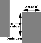
- maxW and minLen control the use of spacing rules in the presence of long and wide wires.
If
maxW is given, then at least one of the pieces of geometry must be that wide.
If minLen is given, then the length of the common parallel run must be at least that long.
|  |
Here are the possible rules:
- LayerRule is a rule for one or more layers.
In addition to the standard attributes, this rule has one or more layer names to which it applies.
The type of information can be
MINWID (minimum width of the layer),
MINAREA (the minimum area of the layer),
MINENCLOSEDAREA (the minimum area of any hold in a polygon),
SURROUND (minimum extension of a layer beyond another),
DIAGONALVIA (diagonal via rules), or
G0CPL (G0 rules).
Example:
   <LayerRule ruleName="1.1 Mosis" layerName="{P-Well, N-Well}" when="ALL"

      type="MINWID" value="12.0"/>
- LayersRule is a rule for the interaction of two different layers.
In addition to the standard attributes, it has the names of the two layers.
The type of information can be
CONSPA (minimum spacing of two connected layers),
UCONSPA (minimum spacing of two unconnected layers),
SPACING (minimum spacing in both connected and unconnected situations),
UCONSPA2D (minimum spacing of a two-dimensional array of contact cuts),
FORBIDDEN (disallowed combination of layers anywhere in the design),
EXTENSION (minimum overlap of a layer extended from another),
SURROUND (minimum extension of a layer beyond another),
DIAGONALVIA (diagonal via rules), or
G0CPL (G0 rules).
Example:
   <LayersRule ruleName="15.4 Mosis" layerNames="{Metal-3,Metal-3}"

      when="ALL" type="SPACING" value="6" maxW="100" minLen="0"/>
- NodeRule gives rules for Electric nodes.
In addition to the standard attributes, it has a node name.
The type of information can be
NODSIZ (the minimum size of a node),
or
FORBIDDEN (the node is not allowed).
Example:
   <NodeRule ruleName="5.2 Mosis" nodeName="Metal-1-Polysilicon-1-Con"

      when="ALL" type="NODSIZ" value="5"/>
- NodeLayersRule gives rules for specific layers in a single node.
In addition to the standard attributes, it has both layer names and a node name.
The type of information can be
SURROUND (for layers in a node)
or
ASURROUND (for layers in an arc).
Example:
   <NodeLayersRule ruleName="2.3 Mosis" layerNames="{P-Well, N-Active}"

      nodeName="N-Transistor" when="ALL" type="SURROUND" value="5"/>
In addition to design-rules, the GDS layer assignments are also found in the Foundry section.
Each GDS layer line has this format:
<layerGds layer="XXXX" gds="YYYY"/>
Where XXXX is the layer name and YYYY is the GDS information for that layer.
The GDS information can include multiple layer numbers, for example "21,49,98".
GDS layers can have type information if separated by a slash, for example layer 14 type 141 is "21/141".
GDS layers can be used for Pins (export locations) and Text (export names) by appending a "p" or "t" to the layer number,
for example "21,49p,74/2t".
Example:
<layerGds layer="Metal-1" gds="49,80p,80t"/>
<layerGds layer="Metal-2" gds="41/40,141p"/>
<layerGds layer="Metal-3" gds="98"/>
Defines Metal-1 to be on GDS layer 49, or 80 for pins or text; defines Metal-2 to be on GDS layer 41, type 40 or on layer 141 for pins;
and defines Metal-3 to be on GDS layer 98.


